Calculation of press-fit contacts
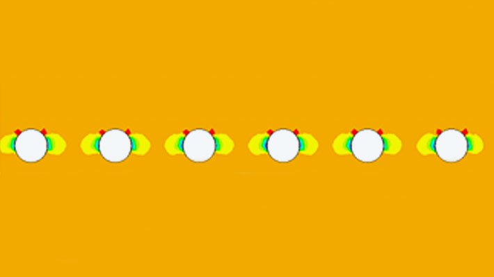
Sector: Electrical engineering/electronicsSpecialist field: Structural mechanicsAB Elektronik GmbH is an automotive supplier for electromechanical products. For the special process of press-fit technology for the solder-free connection of components on printed circuit boards, the strain distribution was analyzed using simulation.
Summary
Task
The task was to determine the strain distribution in a printed circuit board formed after the press-fit of ERNI contacts.
Solution
Ansys simulation tools were used to reproduce the through-hole plating in the model, as well as the elastoplastic material behavior of the printed circuit board.
Customer benefits
AB Elektronik GmbH used the findings from the simulation for optimal positioning of the electronic components on the printed circuit board. Simulation ensures that the press-fit process is performed without damage.
Project Details
Task
The press-fit technique is a special connection technique for electronic circuit boards to make solderless electrical connections. For this purpose, a press-fit pin must be pressed into the metallized hole (through-hole) of a printed circuit board. The essential feature here is that the diagonal of the pin cross-section is larger than the diameter of the hole in the PCB. The strain distribution in a printed circuit board formed after pressing in ERNI contacts was to be determined.

Customer Benefit
The calculated strain distribution enables the designer to position the electronic components optimally on the printed circuit board. The results of the computational simulation can be used to ensure that the sensitive components are not damaged during the press-fit process.

Solution
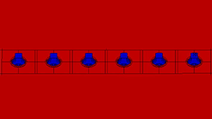
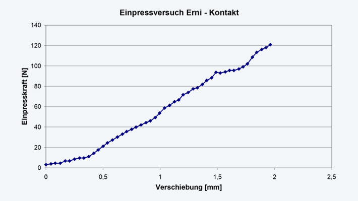
Since this is a very complicated and computationally intensive process, calculations for the ERNI contact were first carried out on a half model. Within this calculation, the coefficient of friction between the vias was optimized so that the required press-in force matched the result from the test as closely as possible. The printed circuit board is calculated with a linear-elastic material behavior. The contacting and the Erni contact are calculated with an elastoplastic material behavior. After the preliminary study on the half model, the parameters were transferred to the overall model and the entire system was calculated.

Images: © AB Elektronik GmbH


