Tech Article | 23/04
EMC Troubleshooting at PCB Level Using Ansys SIwave
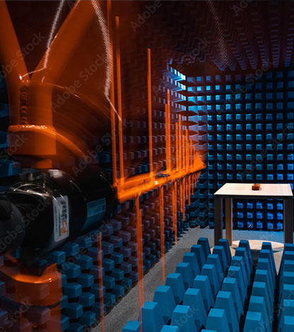
Every electronic device has to pass electromagnetic compatibility (EMC) tests in order to get certified and be brought on market. These EMC tests frequently fail due to radiated emissions, that are measured in many common test standards (e.g. CISPR [EMCSTD]). Radiated emissions often have their root cause in unintended antenna-like resonating structures on the electronics device printed circuit board (PCB).
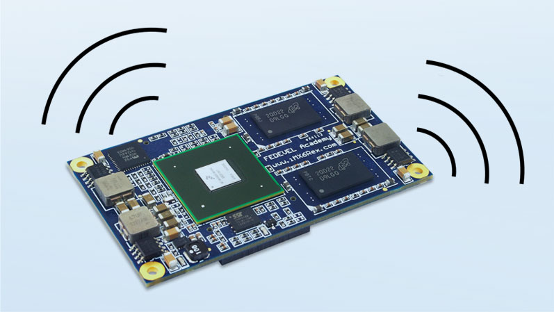
What are antenna-like structures on PCBs?
Everyone might have seen structures declared as “antennas”. Consider the classical rod antenna, you may see at some car roofs. These antennas have the function to receive high-frequent signals from the air, sent by any transmitters also via antennas, and route them to any further detecting and decoding unit. The rod itself works – together with other electronic components – as a resonating structure for high-frequent currents flowing through, resulting in a standing wave. The currents interact with the surrounding space being the source of electromagnetic waves or – speaking of a reciprocal system - incoming electromagnetic waves would induce corresponding currents. You may wonder, why you cannot find an antenna when looking at your smartphone, which is obviously a transceiver system for such waves. What determines the shape of an antenna?
Going back in days, antennas were large structures. Even the first mobiles had little rods at their side. This gives us a clue, that geometric dimension might influence the potential to radiate. Indeed, the antenna’s length is an important factor for its resonance frequency, where the antenna has the highest potential to radiate. As a rule of thumb, we can say the longer the antenna is, the lower is its first resonance frequency. But there are other factors as well, like inductances in series with the antenna arms or capacitances in parallel. Antenna engineers effectively use these additional components to tune antennas and to make their geometric size smaller for integration into devices. The antenna has not necessarily to look like a rod but can also be a folded conductor structure like a copper trace or plane on a PCB with well-defined shape.
This is the crucial point when coming to PCB layouts. You find hundreds of conductor traces, metallic planes, capacitors, and inductors on modern PCBs. Why should not any of them be part of an antenna structure at any frequency in the wide frequency range relevant in EMC standards?
How to identify antenna structures on your PCB?
As an example, let us consider a typical power supply section at a PCB. You may find there a voltage regulator module (VRM), e.g. containing a step-down converter with its large output inductance L. For simplicity, the VRM can be modelled as an ideal voltage source, together with its small source resistance RSource. Typically, the VRM output side is connected to metallic planes to be routed to other integrated circuits (ICs), one plane for the supply voltage level and one for the reference level, often called ground (GND). You can think of the two planes being a parallel plate capacitor with capacitance C. Together, RSource, L and C build a parallel resonator as can be seen from Figure 2.
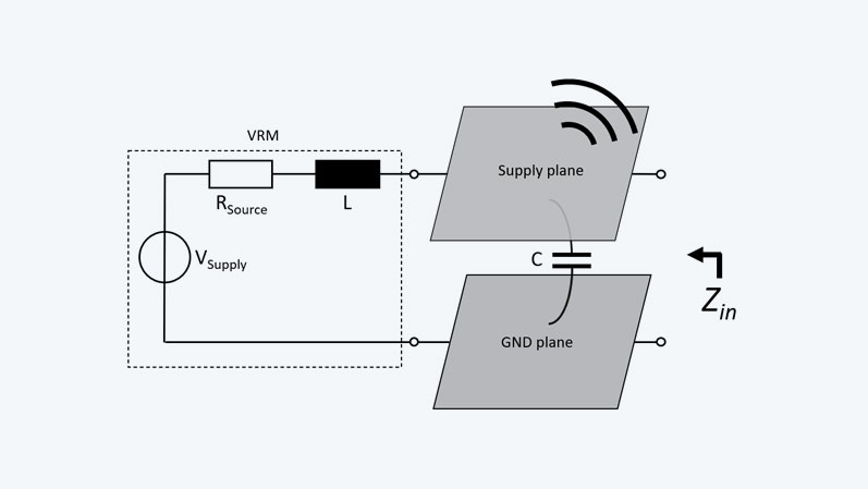
This resonator is nothing else than an antenna structure with tuning components, where the planes take the function of carrying the high-frequent currents as radiation sources, similar to the rod described in the last section. The resonance frequency of a parallel resonator can roughly be estimated to be fres=1 ⁄ (2π√LC)). Due to this relation, the power and ground planes with their large L and C values are most critical to have their resonances at low frequencies in the MHz- to low GHz-range, where many EMC standards operate.
When measuring the input impedance Zin of such a parallel resonator, one might see the low value of RSource for “zero frequency” (DC). The impedance will increase going up in frequency f due to the inductance
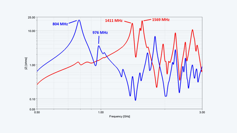
(Zind~fL) and will decrease above the resonance frequency due to the capacitance (Zcap~1/(fC)) In effect, at resonance, a peak value can be seen in the impedance profile. Figure 3 shows a typical impedance profile, measured between a supply and the GND plane of a PCB at two different positions. The position of impedance measurement is relevant to the height of the impedance peak to be seen, but not on the resonance frequency itself. The reason for this is the spatial current and voltage distribution on the planes due to the standing wave in this resonant system.
Why to use simulation software for identifying resonances?
In the last section we showed one way to determine resonant structures by measuring the impedance profile. In a real measurement setup, the positions at a PCB to be reached by a probe tip are very limited. In general, the measurement range is limited to the top and bottom layers. Using a full-wave simulation software, one is able to put measurement probes anywhere within the PCB structure, imported in forms of ECAD data containing the PCBs geometry (e.g., signal traces, planes, substrates) and components like R, L and C. This way, the impedance can even be measured between inner layers of a multilayer PCB.
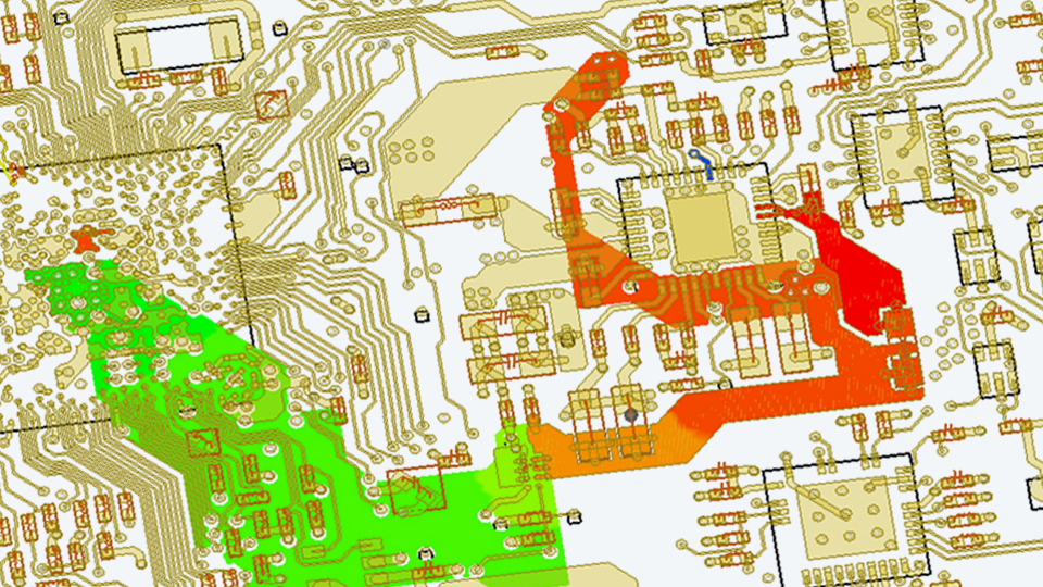
State-of-the-art simulation software like Ansys SIwave [SIWAVE] even contain visualization tools for the voltage and current distributions of resonances. Since being simple to use, more or less one-click-solutions, these tools make it easy to check for resonant structures and to derive optimization methods. Figure 4 shows the voltage distribution between two of the inner PCB layers, corresponding to the resonances marked in the impedance profile can be seen from Figure 3. From the results one can exactly identify, where critical planes contributing to radiated emissions are in the layout.
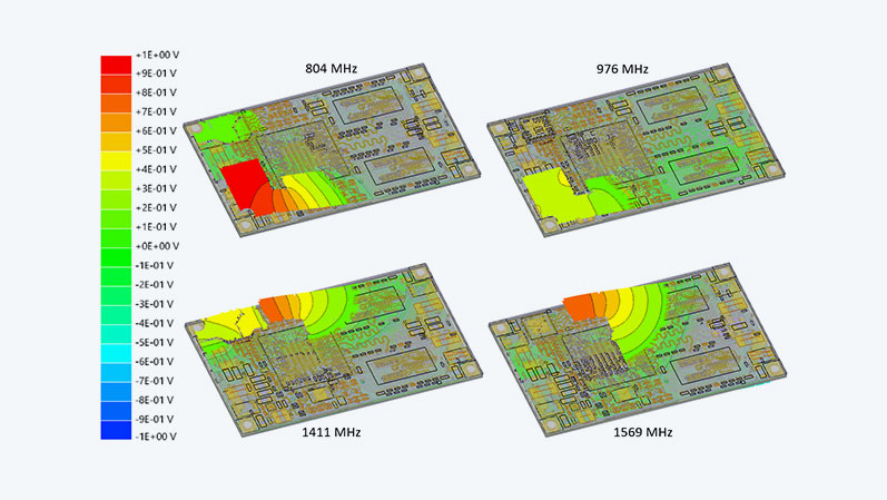
The resonant modes only show the potential to radiate, or – in other words – they identify potential antennas. For radiation, these antennas must be driven by signals. There have to be coupling structures to these antennas on the one hand, and on the other hand, these coupling structures have to carry signals containing spectral components around resonance frequencies. Coupling structures could be for example transmission lines routed nearby to the resonant planes or vias routed through the resonating planes. The spectral components driving the antennas can usually be found in any pulsed signals (e.g., bit-pattern or clock-signals), due to their short rise- and fall times. That’s why the preferred optimization approach should be to eliminate the root-cause of EMC issues, which are the antenna structures in layouts.
Deriving optimization methods from simulation results
With knowledge about the antenna structures in the PCB layout – either by simulated impedance profile or a resonant mode analysis – we have a good starting point for optimization. There are two approaches. Either you can dampen resonances by adding a resistive component (e.g., a real resistor or the equivalent resistance of a capacitor), or you can shift the resonance by changing the L or C values. From an antenna engineer’s point of view, you would detune your antenna. One idea could be to directly cut the length of the resonating antenna arms (in our case planes), by electrically shortening. In case of equipotential planes (e.g., two GND planes) this works by simply adding so called “stitching vias”. From the circuit designer’s point of view this corresponds to decreasing the loop inductance, so decreasing the L value and shifting up the resonance.
For shortening planes of different electric potential (e.g., a supply plane against a GND plane) vias would not be a good idea, since the planes should be kept separated for DC. For a pure AC short, so called “decoupling capacitors” can be chosen. Placing them near to the voltage level maxima of the resonant modes would eliminate the resonance, what can be seen in a resonance frequency shift towards higher frequencies, even out of the EMC test measurement range.
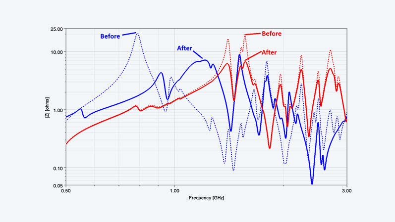
Figure 5 shows the impact of both variants (detuning and dampening) on the impedance profile. In case of detuning (blue curve), the corresponding peaks get shifted to higher frequencies. The whole profile changes due to the different effect on different resonances and due to changing their voltage and current distributions measured by ports. In case of dampening by a resistive value (red curve), the peaks get flattened slightly, but the peaks do not change their frequencies.
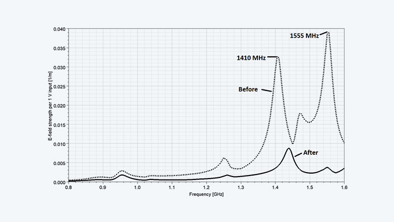
Figure 6 shows the simulated electric field strength in far-field, caused by resonances at the shown PCB. The resonances are driven with 1 Volt at each frequency in the simulation. There can be seen some peaks in field strength. These peaks lay around the simulated resonance frequencies that can be seen from Figure 3. Especially the two modes above 1 GHz strongly contribute to radiated emissions. With the quick optimization approach, the observed field strength can be significantly reduced.
In EMC test standards there are limits specified for this electric field strength, measured by an antenna in a certain distance depending on the standard. The specific values of these frequency dependent limits also vary with the standards. There are standards defined for household devices [EMCSTD] or consumer electronics as well as for industrial or medical equipment [CISPR]. What they all have in common is, that peaks like the ones can be seen from Figure 6 make EMC tests defined there usually fail.
The shown optimization approach by using simulation helps getting rid of the resonances and so of peaks in the EMC measurement. Using simulations like the resonant mode analysis synchronously to your layouting process makes you pass the EMC testing and lets you avoid cost and time intensive remanufacturing cycles. Regarding EMC, you may follow the motto “prevention is better than cure” in your design process.
Author

Published: August 2023
Editorial
Dr.-Ing. Marold Moosrainer
Head of Professional Development
Cover images
Right: © Adobe Stock
Left: © [IMX] www.imx6rex.com
References
[EMCSTD] Electromagnetic compatibility – Requirements for household appliances, electric tools and similar apparatus, Part 1: Emission, International Standard CISPR 14-1, Edition 7.0, September 2020.
[SIWAVE] www.cadfem.net/de/en/our-solutions/ansys-simulation-software-the-product-family/ansys-electromagnetics/ansys-siwave.html
[CISPR] International Standard CISPR 11: Industrial, scientific and medical equipment – Radio-frequency disturbance characteristics – Limits and methods of measurement, Edition 6.0, June 2015.


