Robust design for printed circuit board contacting
Reduce dye-and-pry experiments with simulations
Systems with high computing power often use devices in ball grid arrays (BGA). Right from the development phase, BGAs require robust design and optimization to ensure that they contact the PCB reliably. In this context, soldering results can be improved by simulations.
Simulations instead of dye-and-pry experiments
Ball Grid Arrays (BGA) are integrated circuits with very many connections. Soldering them reliably onto a printed circuit board is a major challenge. This is due to the different coefficients of thermal expansion (CTE) between the component, solder, copper pad and PCB. This causes the materials to deform when they are first heated and then cooled during the soldering process. This can cause cracks to form along the intermetallic phase of the solder joint. How reliable a solder joint is is determined primarily by how much a product is thermally stressed and the metallurgy of the joint. In addition to these environmental factors, the creep behavior of the solder alloy also affects reliability.
Typically, board manufacturers use so-called dye-and-pry experiments to optimize manufacturing parameters. For dye-and-pry, an entire series of boards is first manufactured with different process parameters. The assembled boards are then placed in a bath of a highly viscous, colored liquid (dye). Due to the capillary effect, this liquid penetrates into the microscopically fine cracks that have formed due to the temperature stress, for example in the solder balls of the BGA. The components are then mechanically pried off the boards and the interfaces are examined for cracks, which is, of course, greatly facilitated by the colored liquid in the cracks.
This destructive process is a real battle of materials, which involves high costs. Internal calculations by Zollner show that the experimental effort costs about 45 times more than a simulation. The aim of the following investigation was therefore to find out whether the manufacturing parameters can also be optimized non-destructively by simulation.
Real world and simulation match
After a substitute model is created in Ansys Workbench, the thermal boundary conditions are applied in the form of a reflow solder profile (saddle profile in this case). The viscous and plasticity effects of the solder can be represented by the Anand model [1] in order to model creep as the primary damage mechanism of solder joints. The Ansys Sherlock tool already provides comprehensive insights here at the PCB level. Here, in the first step, lifecycle estimates facilitate the identification of critical components.
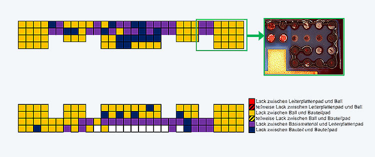
As a result of the simulation and for the quantification of the damage, the creep strain energy density (CSED) is used. This can be determined using a customized Ansys Parametric Design Language (APDL) script. The following figure compares the experimental results from the dye-and-pry tests and the CSED from the simulation. It can be seen well that real and numerical world match to a large extent and critical connections as well as deflection of component and PCB become visible. Additionally, the lifecycle of the entire assembled board was predicted in order to identify further critical components.
Predictive analysis at the solder ball level
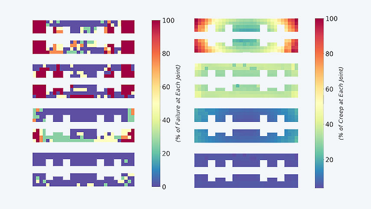
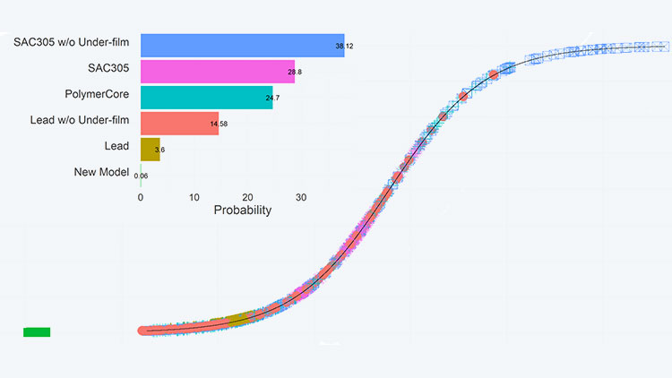
Logistic regression is used to combine the experimental results with the calculated CSED values (as the independent variable) from Ansys Workbench to produce a predictive analysis at the solder ball level. To check how good this fit is, a likelihood ratio test was initially used. This hypothesis test can be used to compare the goodness-of-fit of two models (an unconstrained model whose parameters are all free, and the corresponding model constrained to a few parameters by the null hypothesis) to the sample data. McFadden's Pseudo-R² correlation coefficient is a measure of the variance of each predictor (the variable used to predict a characteristic) for the dependent variable. This serves as another quality measure for the model. The Wald test can be used to statistically test the predictors to see how important each is to model quality.
Finally, the statistical models are analyzed using the ROC (Receiver Operating Characteristic) curve. The area under this curve (AUC) determines which model is ultimately used for the predictive analysis.
Simulation for a design suitable for production
Many influencing factors (e.g. torsion/warping, material mix, solder alloy, etc.) play a major role in the production of printed circuit boards. The experimental results of the dye-and-pry test and the calculated creep strain energy density (CSED) from Ansys are largely in agreement. This makes it possible to develop a predictive model for failure probabilities during the soldering process. Simulation can thus replace cost-intensive experiments to a large extent here.
How the results found are to be implemented in practice is still being evaluated. For example, new rules for the production-oriented design of printed circuit boards are conceivable - keyword “Design for Manufacture”.
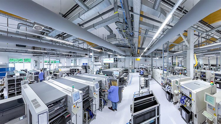
Complex mechatronic systems, from development to after-sales service: As a partner of globally operated top companies as well as small and medium-sized enterprises, Zollner Elektronik AG offers cross-industry system solutions along the entire product life cycle.
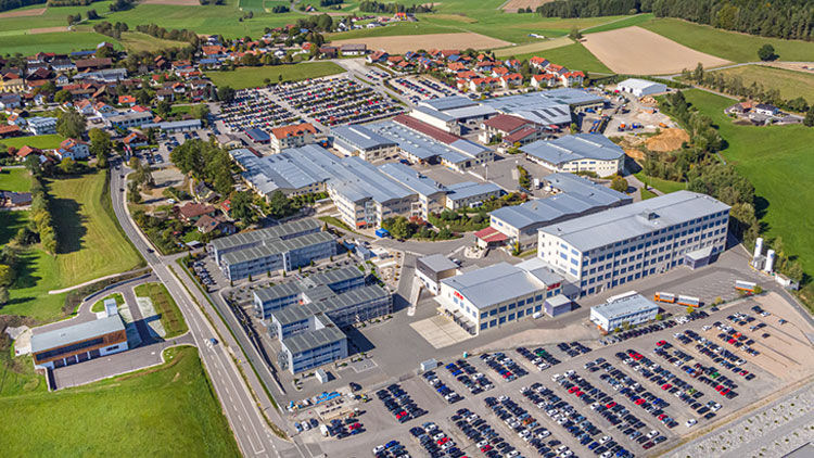
The company was founded in 1965 in Zandt, Bavaria, and is now a public limited company that is 100% family-owned. Through continuous organic growth, the Zollner Group of Companies has established itself as a mechatronics service provider among the top 15 EMS service providers worldwide.
Individual, personal support is important to us - it begins with holistic consulting and continues through all phases of cooperation.
At 20 locations in Germany, Hungary, Romania, China, Tunisia, the USA, Switzerland, Costa Rica and Hong Kong, we focus on quality, an optimal price-performance ratio, technological leadership and a best-cost-country strategy along the entire value chain. Regardless of whether we are dealing with individual parts, modules, equipment or complex systems: The customer decides on the process depth.

Zollner Elektronik AG
Manfred-Zollner-Str. 1
93499 Zandt
www.zollner.de
Authors:
Philemon Olaleru (Zollner Elektronik AG),
Dr. Tim Weber (Zollner Elektronik AG),
Prof. Dr. Peter Firsching (Technische Hochschule Deggendorf)
Referencen:
[1] Anand, L. (1985). Constitutive equations for hot-working of metals. International Journal of Plasticity, 1(3), 213–231. doi.org/10.1016/0749-6419(85)90004-X
First published: Design&Elektronik, 02/2021
www.design-elektronik.de
Contact CADFEM


